
Platings > technologies in Jisso
Plating technologies in Jisso field
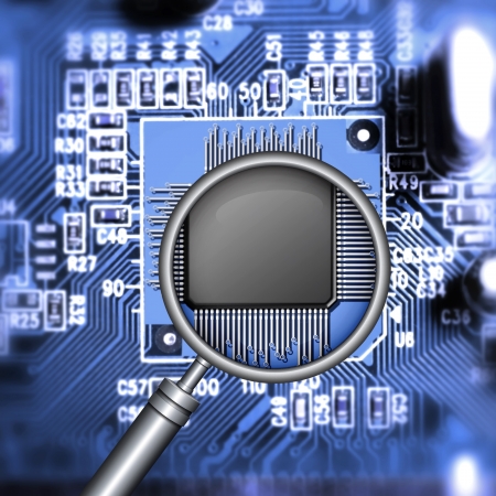
"Jisso" contains many meanings in Japanese. That is, it includes all techniques for shaping parts and devices in soldering, bonding, packaging, assembling and other electronics related. Electronic components are strongly required to be small, highly functional, highly reliable, and lower cost, and plating technology has contributed to these requirements. We introduce the plating technologies related to "Jisso" by Mitsuya.
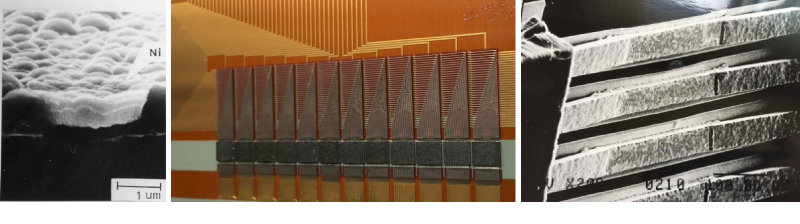
Left:
Multi-layer aluminum wiring formed on a silicon wafer is joined by electroless nickel plating.
Y. Harada, et al., J. Electrochem. Soc., Vol.133, No.11, pp2428-2430(1986)
Center and Right:
IC is connected to the fine wiring formed on the polyimide by TAB (Tape Automated Bonding). Fine wiring: 115μm pitch-electroless nickel + electro copper + electro nickel + electro gold.
H.Sawai, et al., J. Electrochem. Soc., Vol.137, No.11, pp3653-3660 (1990)
Inside ICs
The achievements of Mitsuya are as follows.
- Mass production of a copper pillar bump plating on special 4-inch wafers.
- Successful prototyping of a gold tin bump on 300 mmφ silicon wafer.
The copper pillar bump was plated at a height of 25±5μm.
For gold tin plating on φ300mm wafers, plating thickness and deposit composition are uniform.
The thickness target is about ±20%, and the deposit composition is ±5wt% of the eutectic composition.
Plating could be performed on the patterned circuit (L/S = 50μm/50μm).
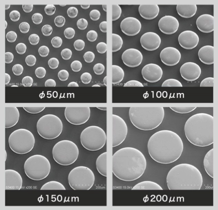
Copper pillar bump at a height 25±5μm
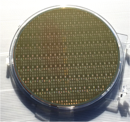
Uniform thickness & uniform composition on φ300mm Wafer
Connection between IC and circuit board
The IC exerts its function once it is connected to an external circuit. There are two methods of connecting ICs, one is using a package and the other is connecting with a bare chip.
The bare chip connection includes wire bonding, TAB (tape automated bonding) and FC (flip chip) bonding.
Mitsuya offer a gold plating suitable for wire bonding. In addition, bump plating for FC is also carried out. We also support such customers as using interposer - substrates.
Terminals and connectors
Characteristics required for the terminal and connector plating are electric conductivity, corrosion resistance, abrasion resistance, and insertability.
Mitsuya offer the plating by gold, silver, palladium, indium, rhodium, nickel etc. for the terminals and the connectors according to customer's request.
The plating method is selected from rack, reel-to-reel, mesh basket based on the shape of the product, plating specifications.
Inspection parts
Along with high density and high performance of ICs, high density and high performance are also required for inspection parts.
Mitsuya plating technologies are used for the probe cards and probe pins to test the characteristics. Especially, a reliable contact with the wafer electrode is important for probe pins corresponding to high-speed and high-frequency, so Mitsuya's high temperature high strength solder plating is used.